Looking for a manufacturing partner for Semiconductor Equipment? VT machining serves the Semiconductor sector with precision metal parts made to specification. Semiconductor tooling requires ultra-clean, ultra-precise parts in specialised alloys with exacting flatness and surface quality.
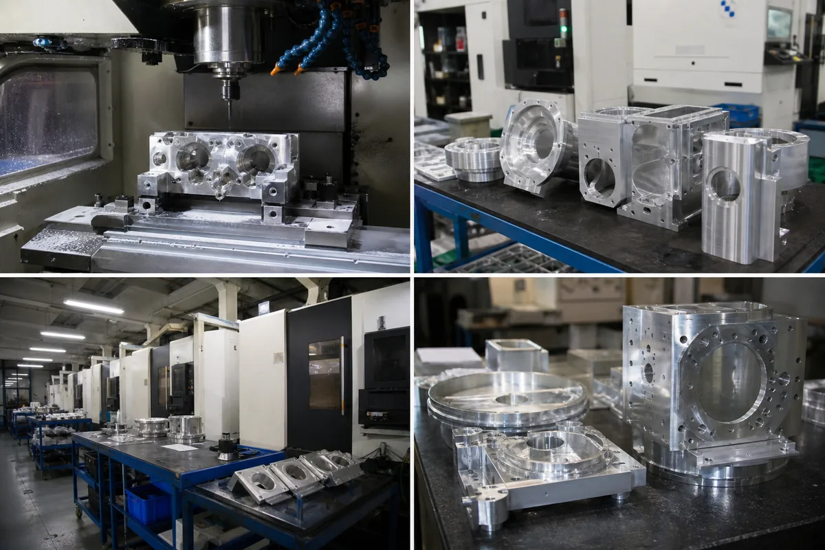
Typical Semiconductor Equipment We Manufacture
- Vacuum-chamber components
- Wafer-handling parts
- Precision electrodes
- Etched grids and masks
- Gas-distribution plates
Components We Build for Semiconductor
Representative jobs with the material, size, driving callout and typical volume. Use it to judge whether your part is in our range before you spend time preparing an RFQ.
| Component | Material | Size | Driving callout | Typical volume |
|---|---|---|---|---|
| Vacuum chamber flange | 6061-T6 aluminium | Ø250 × 25 mm | Sealing face Ra 0.4 µm, flatness 0.010 mm | 120 / year |
| Wafer-handling arm | Ti Gr 2 / 5052 | 400 × 80 × 6 mm | Flatness 0.05 mm, particle-controlled clean | 200 / year |
| Gas distribution plate | 316L stainless | Ø200 × 12 mm | 1,200 × Ø0.5 mm holes, ±0.02 mm | 80 / year |
| Precision electrode | Molybdenum | Ø60 × 8 mm | ±0.010 mm, Ra 0.2 µm | 300 / year |
| Etched grid / mask | Invar 36, 0.1 mm | 150 × 150 mm | Aperture 0.15 ±0.015 mm, stress-relieved | 400 / year |
Processes for Semiconductor Equipment
These VT machining processes are most commonly used to produce Semiconductor Equipment. Follow any link for process capability and material options.
Common Materials for Semiconductor Equipment
Typical alloy families for Semiconductor Equipment. Each links to the relevant process and material capability.
Recommended Grades for Semiconductor Equipment
Specific alloy grades we frequently machine for Semiconductor Equipment. Each links to detailed process-and-grade capability.
Industry Requirements for Semiconductor Equipment
Components for the Semiconductor sector carry real responsibility — they must perform reliably in service. Dimensional accuracy, verified material, clean surface condition and documentation all matter as much as the part itself.
Our quoting and planning for Semiconductor Equipment start by identifying the critical-to-function features. We confirm critical dimensions, material specification and any sector-specific needs before cutting metal, and flag anything that would benefit from a design discussion.
Standards, Documentation & Testing
What Semiconductor buyers normally specify, and what we supply with the shipment. Anything on this list can be added to an order — tell us at RFQ stage so it is priced in rather than bolted on.
| Requirement | How we handle it |
|---|---|
| Cleanliness | Ultrasonic clean, DI rinse, IPA wipe, then double vacuum bagging in a controlled area. |
| Contamination | No silicone, no chlorinated solvents, dedicated tooling for vacuum-service parts. |
| Surface finish | Sealing and vacuum faces measured and reported, typically Ra 0.4 µm or better. |
| Material certificate | EN 10204 3.1 with alloy verification by PMI where the drawing requires it. |
| Dimensional report | CMM report on every nominated feature, per part or per lot as specified. |
| Handling | Gloved handling from final machining onward; no bare-hand contact. |
Design & Manufacturing Considerations
Choosing how to make a Semiconductor Equipment component is a balance of geometry, accuracy and quantity. Depending on the design we use CNC Grinding, Chemical Etching, CNC Milling, CNC Drilling, CNC Tapping, CNC Reaming, often combining several in one workflow.
Sharing your 3D model early lets us return practical design-for-manufacture feedback. Adjusting corner radii, datum strategy or non-critical tolerances frequently improves manufacturability at no functional loss.
Quality, Inspection & Compliance
We treat quality as part of manufacturing Semiconductor Equipment, not a final gate. Critical dimensions are checked in-process and confirmed at final inspection with calibrated instruments, with CMM measurement where tolerances demand it.
Documentation typical of Semiconductor programmes — mill certs, inspection reports, FAIR — is available on request. We adapt our quality documentation to the standards your application requires.
Why Choose VT machining for Semiconductor Equipment
VT machining brings broad in-house capability to Semiconductor Equipment, from one-off parts to repeat production. Machining, grinding, EDM, cutting, forming, finishing and inspection are managed under one roof, which shortens lead times and keeps quality consistent.
Share your model, material, quantity and quality needs. We reply quickly with price, lead time and honest manufacturability notes.
No drawing yet? Build one in the browser.
Set the metal, dimensions and features, watch the 3D model update as you type, then switch to the 2D sheet to add dimensions and tolerances. Download it or send it straight to us with your RFQ.
What We Need to Quote Semiconductor Equipment
- GeometrySTEP or IGES for the 3D model, plus a PDF drawing if you have tolerance callouts. A dimensioned sketch is enough to start.
- MaterialThe exact alloy, grade and condition — temper, heat-treat state or hardness. If you are not sure, tell us the function and we will suggest one.
- QuantityPrototype count and the expected annual volume. Both change how the part is made and therefore what it costs.
- TolerancesWhich features are critical. Everything else runs to our standard tolerance, which is what keeps the price sensible.
- FinishSurface treatment, cosmetic requirements, and any faces that must be masked.
- DocumentsWhether you need a material certificate, dimensional report, FAIR or PPAP with the shipment.
Missing something from the list is not a problem — send what you have. We will come back with the specific questions rather than a generic form.
Send the drawing, the material and the quantity. Pricing, lead time and DFM notes come back — usually within one business day.
Request a QuoteFrequently Asked Questions
What does VT machining produce for Semiconductor Equipment?
VT machining produces precision metal parts for Semiconductor Equipment in the Semiconductor sector, including vacuum-chamber components, wafer-handling parts, precision electrodes, etched grids and masks. Every part is manufactured to your CAD or 2D drawing, with the process and material selected to suit your tolerance, finish and volume requirements.
Do you handle prototypes and production volume for Semiconductor Equipment?
Yes. We support Semiconductor Equipment programs from a single prototype through to ongoing production. Send your drawing and quantity for feasibility, pricing and lead time.
Which processes are used for Semiconductor Equipment?
We commonly use CNC Grinding, Chemical Etching, CNC Milling, CNC Drilling, CNC Tapping, CNC Reaming for Semiconductor Equipment. The right route is chosen per part — share your geometry and tolerance and we will confirm the optimal process and any secondary operations.
What materials are typically used for Semiconductor Equipment?
Common materials for Semiconductor Equipment include Aluminum, Molybdenum, Tungsten, Stainless Steel. We work across a wider machining metal set on request; tell us the alloy and grade you need and we will confirm capability.
How do I get a quotation for Semiconductor Equipment?
Send your CAD model or 2D drawing, the material/grade you need and your quantity. Our engineers usually reply within one business day with feasibility, lead time and pricing.